| CPC H10K 39/32 (2023.02) [H10K 85/221 (2023.02)] | 12 Claims |

|
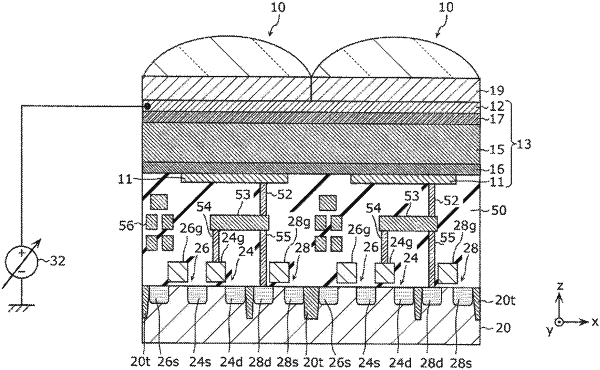
1. An imaging device comprising:
a plurality of pixels, wherein;
each of the plurality of pixels includes a counter electrode that passes incident light, a pixel electrode that faces the counter electrode, and a photoelectric conversion layer that is located between the counter electrode and the pixel electrode and that includes carbon nanotubes,
the plurality of pixels include a first pixel and a second pixel adjacent to the first pixel,
the pixel electrode of the first pixel and the pixel electrode of the second pixel are isolated from each other,
the photoelectric conversion layer is continuously provided between the first pixel and the second pixel, and
the carbon nanotubes included in the photoelectric conversion layer in at least one selected from the group consisting of the first pixel and the second pixel include at least one first carbon nanotube that satisfies A<B, where A denotes length of one carbon nanotube of the carbon nanotubes in a direction in which the pixel electrode of the first pixel and the pixel electrode of the second pixel are arranged and B denotes length of a gap between the pixel electrode of the first pixel and the pixel electrode of the second pixel.
|