| CPC H10B 43/40 (2023.02) [G11C 16/08 (2013.01); G11C 16/24 (2013.01); G11C 16/30 (2013.01); H10B 43/20 (2023.02); H10B 43/35 (2023.02)] | 9 Claims |

|
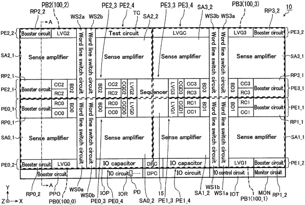
1. A semiconductor memory device comprising:
a first plane including:
a first memory cell array provided above a substrate in a first direction and including a plurality of first memory cells, the first direction intersecting a surface of the substrate;
a first power supply circuit provided between the substrate and the first memory cell array and configured to output a first voltage to be applied to the first memory cells; and
a first sense amplifier provided between the substrate and the first memory cell array and having a finer design rule than the first power supply circuit; and
a second plane including:
a second memory cell array provided above the substrate in the first direction and including a plurality of second memory cells;
a second power supply circuit provided between the substrate and the second memory cell array and configured to output a second voltage to be applied to the second memory cells; and
a second sense amplifier provided between the substrate and the second memory cell array and having a finer design rule than the second power supply circuit,
wherein, when viewed in the first direction, the first power supply circuit and the first sense amplifier overlap the first memory cell array, and the second power supply circuit and the second sense amplifier overlap the second memory cell array.
|