| CPC H10B 43/27 (2023.02) [H01L 24/08 (2013.01); H01L 24/80 (2013.01); H01L 25/0657 (2013.01); H01L 25/18 (2013.01); H01L 25/50 (2013.01); H10B 41/27 (2023.02); H01L 2224/08145 (2013.01); H01L 2224/80895 (2013.01); H01L 2224/80896 (2013.01); H01L 2924/1431 (2013.01); H01L 2924/14511 (2013.01)] | 15 Claims |

|
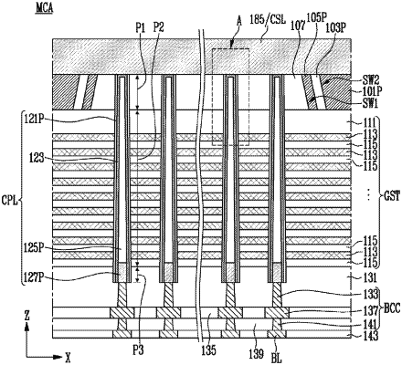
1. A semiconductor memory device comprising:
a bit line;
a common source pattern above the bit line;
a channel layer in contact with the common source pattern, the channel layer extending toward the bit line;
a filling insulating layer disposed between the bit line and the common source pattern, the filling insulating layer surrounding a first part of the channel layer;
a gate stack structure disposed between the bit line and the filling insulating layer, the gate stack structure surrounding a second part of the channel layer;
a first etch stop pattern on a sidewall of the filling insulating layer;
a second etch stop pattern between the first etch stop pattern and the filling insulating layer; and
a memory pattern between the gate stack structure and the channel layer,
wherein a first sidewall of the second etch stop pattern which is in contact with the filling insulating layer and a second sidewall of the second etch stop pattern which is in contact with the first etch stop pattern are inclined in the same direction.
|