| CPC H10B 43/27 (2023.02) | 20 Claims |
|
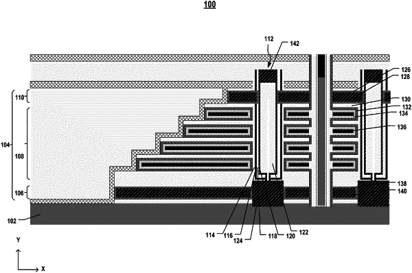
1. A three-dimensional (3D) memory device, comprising:
a doped semiconductor layer;
a stack structure comprising interleaved conductive layers and dielectric layers formed on the doped semiconductor layer, the conductive layers comprising a plurality of word lines, and a drain select gate line; and
a channel structure comprising a semiconductor channel and a memory film over the semiconductor channel, the channel structure extending through the stack structure along a first direction and in contact with the doped semiconductor layer,
wherein the drain select gate line comprises a first dielectric layer in direct contact with the semiconductor channel of the channel structure, and a first polysilicon layer in contact with the first dielectric layer.
|