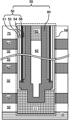
| CPC H10B 43/27 (2023.02) | 19 Claims |

|
1. A memory device, comprising:
an alternating stack of insulating layers and electrically conductive layers located over a substrate;
a memory opening vertically extending through the alternating stack; and
a memory opening fill structure located in the memory opening,
wherein:
the memory opening fill structure comprises a memory film and a vertical semiconductor channel that comprises a cylindrical portion that vertically extends through at least a topmost one of the electrically conductive layers and a bulging portion that is adjoined to a bottom end of the cylindrical portion and having a greater lateral extent than the cylindrical portion;
the memory film comprises a tunneling dielectric layer, a charge storage layer that laterally surrounds the tunneling dielectric layer, a dielectric metal oxide blocking dielectric layer that laterally surrounds the charge storage layer and contacts the bulging portion of the vertical semiconductor channel, and a silicon oxide blocking dielectric layer that laterally surrounds the dielectric metal oxide blocking dielectric layer;
the tunneling dielectric layer has an inner cylindrical sidewall that directly contacts the cylindrical portion of the vertical semiconductor channel within a first cylindrical vertical plane;
an outer annular region of the bulging portion of the vertical semiconductor channel is located entirely outside the first cylindrical vertical plane, wherein the outer annular region of the bulging portion of the vertical semiconductor channel is in direct contact with an entirety of a bottom surface of the charge storage layer, and wherein a bottom portion of an inner cylindrical sidewall of the silicon oxide blocking dielectric layer is in direct contact with the outer annular region of the bulging portion of the vertical semiconductor channel; and
the charge storage layer has an inner cylindrical sidewall that directly contacts a first cylindrical surface segment of the outer annular region of the bulging portion of the vertical semiconductor channel within a second cylindrical vertical plane that is laterally offset outward relative to the first cylindrical vertical plane by a thickness of the tunneling dielectric layer.
|