| CPC H10B 12/482 (2023.02) [H10B 12/315 (2023.02); H10B 12/34 (2023.02)] | 18 Claims |

|
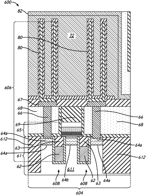
1. An apparatus, comprising:
a conductive base layer including silicon;
a first conductive layer including silicide of a conductive material above the conductive base layer;
a conductive barrier layer above the first conductive layer; and
a second conductive layer above the conductive barrier layer,
wherein the conductive barrier layer has a first thickness that is greater than a thickness of a first precursor conductive layer configured to form at least a lower portion of the conductive barrier layer and that is greater than a thickness of a second precursor conductive layer configured to form at least an upper portion of the conductive barrier layer,
wherein the second conductive layer has a second thickness that is greater than a thickness of a third precursor conductive layer configured to form at least a lower portion of the second conductive layer and that is greater than a thickness of a fourth precursor conductive layer configured to form at least an upper portion of the second conductive layer, and
wherein the second conductive layer includes ruthenium, the third precursor conductive layer includes ruthenium nitride, and the fourth precursor conductive layer includes ruthenium.
|