| CPC H10B 10/12 (2023.02) [G11C 11/412 (2013.01); G11C 11/419 (2013.01)] | 20 Claims |
|
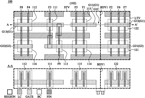
1. A static random access memory (SRAM) device, comprising:
a first gate of a first pass-gate transistor extending to cross a first number of fins in a first threshold voltage region of a substrate; and
a second gate of a second pass-gate transistor extending to cross a second number of fins in a second threshold voltage region of the substrate,
wherein the first gate and the second gate are aligned to each other on a cross-sectional line along a first direction,
wherein a boundary of the first threshold voltage region between the first and second gates is arranged closer to one, which crosses a smaller number of fins, of the first and second gates.
|