| CPC H05K 1/0256 (2013.01) [H05K 1/09 (2013.01)] | 18 Claims |
|
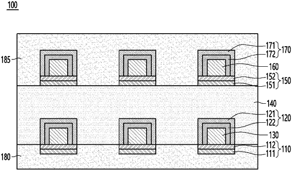
1. A circuit board comprising:
a first protective layer;
a first circuit pattern disposed on the first protective layer;
an insulating layer disposed on the first protective layer and the first circuit pattern; and
a first barrier layer surrounding an upper surface, a side surface and a lower surface of the first circuit pattern and disposed in the first protective layer and the insulating layer,
wherein the first barrier layer includes a first portion disposed in the first protective layer, and a second portion disposed in the insulating layer,
wherein the first portion of the first barrier layer includes:
a first metal layer disposed under the lower surface of the first circuit pattern; and
a second metal layer disposed under a lower surface of the first metal layer and including a metal material different from that of the first metal layer,
wherein the second portion of the first barrier layer includes:
a third metal layer disposed surrounding the side surface and the upper surfaces of the first circuit pattern
and including the same metal material as that of the first metal layer; and
a fourth metal layer disposed surrounding the third metal layer and including the same metal material as the second metal layer.
|