|
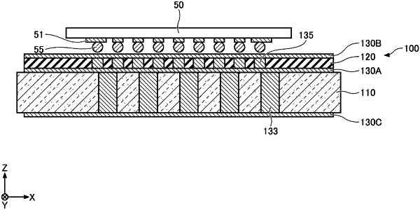
1. A high-frequency circuit board comprising: a first insulating layer having a first dielectric constant; a first metal layer provided to stack over the first insulating layer; a second insulating layer provided to stack over the first metal layer, and having a second dielectric constant lower than the first dielectric constant; a second metal layer provided to stack over the second insulating layer, on which a compound semiconductor device is mounted; and first vias penetrating the second insulating layer and connecting the first metal layer with the second metal layer, further comprising: a third metal layer arranged on an opposite side to the first metal layer with respect to the first insulating layer, and held at reference potential; and second vias penetrating the first insulating layer and connecting the first metal layer with the third metal layer.
|