| CPC H05H 1/46 (2013.01) [H01J 37/32174 (2013.01); H01J 37/32183 (2013.01); H03F 3/2173 (2013.01); H05H 1/4652 (2021.05); H05H 1/466 (2021.05); H05H 2242/10 (2013.01); H05H 2242/24 (2021.05)] | 14 Claims |
|
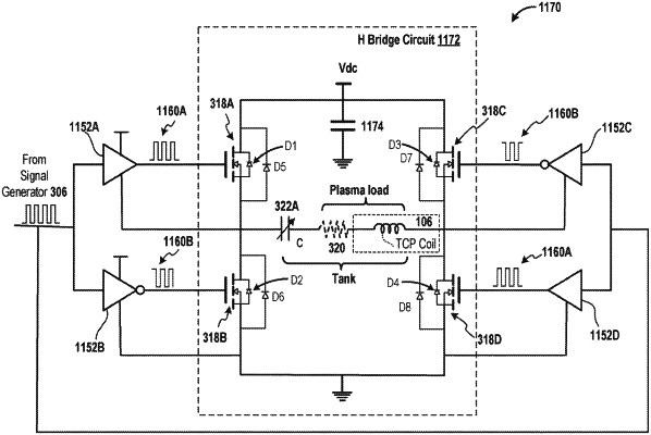
1. A matchless plasma source comprising:
a signal generator configured to generate a square wave signal having a frequency;
a first gate driver coupled to the signal generator, wherein the first gate driver is configured to receive the square wave signal to output a first plurality of reversely synchronized signals having the same frequency as that of the square wave signal, wherein the first plurality of reversely synchronized signals include a first signal and a second signal;
a second gate driver coupled to the signal generator, wherein the second gate driver is configured to receive the square wave signal to output a second plurality of reversely synchronized signals, wherein the second plurality of reversely synchronized signals include a third signal and a fourth signal; and
an H bridge circuit coupled to the first and second gate drivers, wherein the H bridge circuit includes:
a first plurality of transistors including a first transistor and a second transistor, wherein the first transistor is configured to receive the first signal and the second transistor is configured to receive the second signal to output a first waveform;
a second plurality of transistors including a third transistor and a fourth transistor, wherein the third transistor is configured to receive the third signal and the fourth transistor is configured to receive the fourth signal to output a second waveform; and
a reactive circuit coupled to the first and second transistors, wherein the reactive circuit is configured to receive the first waveform to output a sinusoidal radio frequency (RF) signal.
|