| CPC H04N 25/79 (2023.01) [H01L 27/0255 (2013.01); H01L 27/0296 (2013.01); H01L 27/146 (2013.01); H01L 27/14636 (2013.01); H01L 27/1464 (2013.01); H01L 27/14685 (2013.01); H01L 27/14689 (2013.01); H10K 65/00 (2023.02); H01L 27/14645 (2013.01)] | 42 Claims |

|
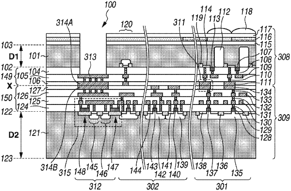
1. A device comprising:
a first semiconductor substrate which includes a photoelectric conversion element;
a second semiconductor substrate which includes a transistor; and
a wiring structure which is arranged between the first semiconductor substrate and the second semiconductor substrate,
wherein the first semiconductor substrate is provided with an opening,
wherein the second semiconductor substrate includes semiconductor regions and an insulating member,
wherein the semiconductor regions include a first semiconductor region and a second semiconductor region separated from the first semiconductor region by the insulating member, and
wherein the opening and at least one of the insulating member, the first semiconductor region and the second semiconductor regions overlap each other, or the opening and a poly silicon portion arranged between the wiring structure and the second semiconductor substrate overlap each other.
|