| CPC H04N 25/771 (2023.01) [H01L 27/14623 (2013.01); H04N 25/42 (2023.01); H04N 25/778 (2023.01)] | 12 Claims |

|
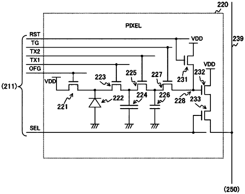
1. A solid-state imaging element, comprising:
a photoelectric conversion element;
a front-stage charge holding region;
a rear-stage charge holding region, wherein a capacity of the rear-stage charge holding region is different from a capacity of the front-stage charge holding region;
a front-stage transfer transistor configured to transfer a first charge from the photoelectric conversion element to the front-stage charge holding region and the rear-stage charge holding region;
a rear-stage transfer transistor configured to transfer the first charge from the rear-stage charge holding region to a floating diffusion region;
an intermediate transfer transistor configured to transfer a second charge, which remains in the front-stage charge holding region after the first charge has been transferred from the rear-stage charge holding region to the floating diffusion region, to the floating diffusion region via the front-stage charge holding region;
a light-shielding wall configured to prevent the first charge to leak from the photoelectric conversion element to the rear-stage charge holding region; and
a signal processing circuit configured to:
compare, between a first pixel signal corresponding to an amount of charge transferred from the rear-stage charge holding region and a second pixel signal corresponding to an amount of charge transferred from the front-stage charge holding region and the rear-stage charge holding region, the first pixel signal with a specific threshold; and
select one of the first pixel signal or the second pixel signal based on a comparison result.
|