| CPC H04N 25/77 (2023.01) [H01L 27/14634 (2013.01); H04N 25/709 (2023.01)] | 20 Claims |

|
1. A solid-state image sensor comprising:
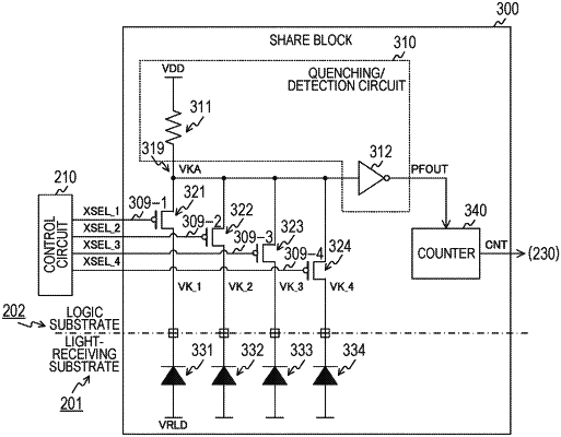
a light-receiving substrate on which a plurality of avalanche photodiodes is disposed, each of the avalanche photodiodes generating a current corresponding to incidence of a photon; and
a logic substrate on which a counter is disposed, the counter counting a number of the photons on a basis of the current of a selected avalanche photodiode among the plurality of avalanche photodiodes, wherein
the plurality of avalanche photodiodes includes first and second avalanche photodiodes, and
there are further disposed, on the logic substrate, a detection circuit that generates a pulse signal on a basis of a voltage according to the current and outputs the pulse signal to the counter, a first selection transistor that opens and closes a path between one end of the first avalanche photodiode and the detection circuit, a second selection transistor that opens and closes a path between one end of the second avalanche photodiode and the detection circuit, and a control circuit that controls a voltage of each gate of the first and second selection transistors.
|