| CPC H04N 19/12 (2014.11) [H04N 19/124 (2014.11); H04N 19/156 (2014.11); H04N 19/157 (2014.11); H04N 19/186 (2014.11); H04N 19/46 (2014.11); H04N 19/61 (2014.11); H04N 19/625 (2014.11)] | 14 Claims |

|
1. An image processing device comprising:
circuitry configured to set an encoding mode of encoding of an image by
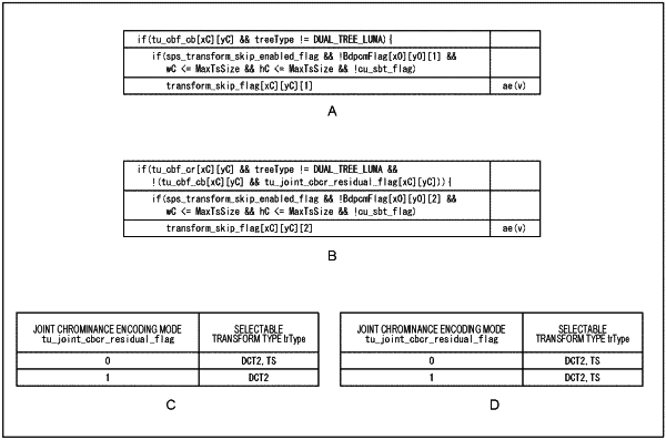
setting a transform type with a minimum encoding cost in a non-joint chrominance encoding mode as a transform type in a joint chrominance encoding mode, and
deriving an encoding cost in the joint chrominance encoding mode, wherein the circuitry is configured to
compare the minimum encoding cost of the non-joint chrominance encoding mode with the encoding cost of the joint chrominance encoding mode, and
select a mode with the minimum encoding cost.
|