| CPC H04L 7/033 (2013.01) [H04L 43/087 (2013.01)] | 20 Claims |

|
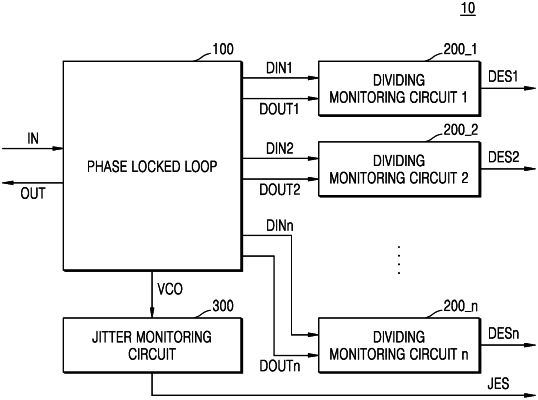
1. A monitoring circuit comprising:
a phase locked loop configured to generate an output signal by dividing an input signal based on a plurality of dividers;
a plurality of dividing monitoring circuits, each dividing monitoring circuit being associated with a respective divider of the plurality of dividers and configured to receive a dividing input signal and a dividing output signal corresponding to the respective divider and to output a dividing error signal based on a dividing ratio range and a dividing ratio of the dividing output signal to the dividing input signal corresponding to the respective divider; and
a jitter monitoring circuit configured to output a jitter error signal based on jitter of a signal generated in the phase locked loop and a jitter error range set in a calibration mode.
|