| CPC H03K 19/018521 (2013.01) [H03K 19/00384 (2013.01)] | 16 Claims |

|
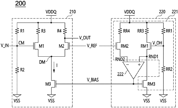
1. An input buffer circuit comprising:
a signal input circuit configured to receive an input signal to generate an output signal based on a reference voltage and an activation current; and
a linear setting circuit configured to compare a voltage of a first modeling node, which corresponds to the input signal, with a voltage of a second modeling node, which corresponds to the reference voltage, to generate a bias voltage for controlling the activation current.
|