| CPC H03K 19/0005 (2013.01) [G11C 7/1048 (2013.01); G11C 16/0483 (2013.01)] | 15 Claims |

|
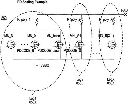
1. A voltage mode driver, comprising:
a pull-down stage including:
a first circuit having a plurality of nMOS devices in parallel, the plurality of nMOS devices being common to a first resistor;
a second circuit in parallel with the first circuit and having an nMOS device in series with a second resistor; and
X-2 additional circuits in parallel with the first and second circuits, each additional circuit having an additional nMOS device in series with an additional resistor,
wherein the second circuit is configured to be enabled when a pulldown impedance of the first circuit, with the second circuit disabled and all of the nMOS devices of the first circuit turned on, is greater than a desired pulldown impedance, and
wherein each of the first circuit through a Yth circuit are configured to be enabled when a condition is met that the pulldown impedance of the first through the (Y-1) th circuits, with the Yth circuit disabled and all of the nMOS devices of the first through the (Y-1) th circuits turned on, is greater than the desired pulldown impedance, and
wherein X is an integer greater than 2, and Y is an integer greater than 1.
|