| CPC H03H 9/02228 (2013.01) [H03H 3/02 (2013.01); H03H 3/08 (2013.01); H03H 9/02031 (2013.01); H03H 9/02637 (2013.01); H03H 9/132 (2013.01); H03H 9/145 (2013.01); H03H 9/175 (2013.01); H03H 9/176 (2013.01); H03H 9/25 (2013.01); H03H 9/562 (2013.01); H03H 9/564 (2013.01); H03H 9/568 (2013.01); H03H 2003/025 (2013.01)] | 20 Claims |

|
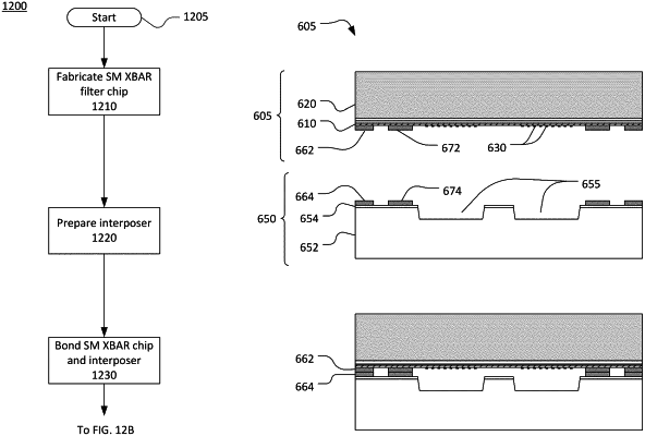
1. A method of fabricating an acoustic resonator device, the method comprising:
fabricating a bulk acoustic resonator chip comprising:
forming a first conductor pattern on a front surface of a piezoelectric layer, the first conductor pattern comprising a first plurality of contact pads and an interdigital transducer (IDT), the IDT and the piezoelectric layer configured such that a radio frequency signal applied to the IDT excites a primary shear acoustic mode in the piezoelectric layer; and
forming an acoustic Bragg reflector between a surface of a substrate and a back surface of the piezoelectric layer, the acoustic Bragg reflector configured to reflect the shear primary acoustic mode;
fabricating an interposer comprising:
forming a second conductor pattern on a surface of the interposer that faces the bulk acoustic resonator chip, the second conductor pattern comprising a second plurality of contact pads;
forming gold bumps by thermocompression or ultrasonic bonding to connect each contact pad of the first plurality of contact pads to a respective contact pad of the second plurality of contact pads; and
forming a polymer cover that is cast over the bulk acoustic resonator chip to seal a space between the bulk acoustic resonator chip and the interposer.
|