| CPC H03F 3/2171 (2013.01) [H03F 2200/03 (2013.01); H03F 2200/372 (2013.01)] | 20 Claims |
|
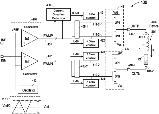
1. A switching amplifier circuit, comprising:
a first output stage, comprising a first pull-up transistor and a first pull-down transistor connected in series at a first output node between first and second reference voltages, each of the first pull-up and pull-down transistors having control terminals and receiving a first differential switching control signal from a switched modulator, the first output node providing a first differential output signal to a first end of a load device;
a second output stage, comprising a second pull-up transistor and a second pull-down transistor connected in series at a second output node between the first and second reference voltages, each of the second pull-up and pull-down transistors having control terminals receiving a second differential switching control signals from the switched modulator, the second output node providing a second differential output signal to a second end of the load device;
a current direction detection circuit coupled to the first output of the switched modulator and the second output of the switched modulator to determine a direction of an output current and provide a current direction signal to indicate if the output current flows from the first output node to the second output node, or the output current flows from the second output node to the first output node;
first, second, third, and fourth slew control circuits, responsive to the current direction signal, and coupled to the first pull-up transistor, the first pull-down transistor, the second pull-up transistor, and the second pull-down transistor, respectively;
wherein:
the first slew control circuit is activated only during turnoff of the first pull-up transistor when the output current flows from the first output node to the second output node;
the second slew control circuit is activated only during turnoff of the first pull-down transistor when the output current flows from the second output node to the first output node;
the third slew control circuit is activated only during turnoff of the second pull-up transistor when the output current flows from the second output node to the first output node; and
the fourth slew control circuit is activated only during turnoff of the second pull-down transistor when the output current flows from the first output node to the second output node.
|