| CPC H03F 3/19 (2013.01) [H03F 1/565 (2013.01); H03F 2200/165 (2013.01); H03F 2200/222 (2013.01); H03F 2200/294 (2013.01); H03F 2200/451 (2013.01)] | 21 Claims |

|
1. A multi-input multi-band low noise amplifier (LNA) comprising:
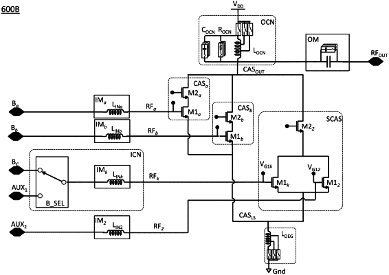
a dedicated RF processing path comprising a dedicated cascode amplifier comprising a dedicated input transistor and a dedicated output cascode transistor that is coupled to a high side node;
a multi-input shared cascode amplifier comprising a plurality of input transistors and a shared output cascode transistor coupled to the plurality of input transistors, the shared output cascode transistor being coupled to the high side node and the high side node being coupled to a supply voltage through a tunable inductor;
a shared RF processing path for processing of at least two respective frequency bands, the shared RF processing path comprising an input band selection switch configured to selectively couple an input RF signal of each of the at least two respective frequency bands to a shared input transistor of the plurality of input transistors;
wherein the high side node is further coupled to the supply voltage through at least a resistor or a capacitor.
|