| CPC H03F 1/0205 (2013.01) [H03F 3/45475 (2013.01)] | 20 Claims |
|
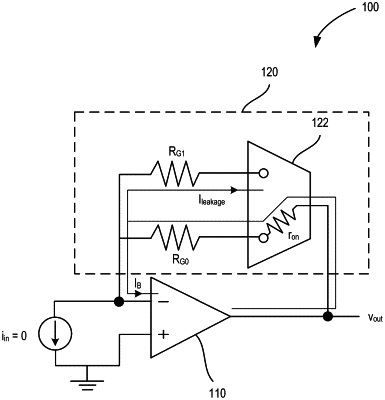
1. A low off-leakage switched gain trans-impedance amplifier (TIA) circuit having an input terminal to receive an input current, the switched gain TIA circuit comprising:
a first switch including a first transistor circuit coupled in series with a second transistor circuit via a first midpoint node, wherein a back-gate node of the second transistor circuit is coupled to the first midpoint node, and wherein the first switch has an ON state and an OFF state;
an amplifier circuit including an output node coupled to an input node of the first switch and an input node of a second switch; and
a bootstrapping circuit configured to receive a voltage and generate an output signal selectively coupleable to the first midpoint node to bias the first midpoint node to a representation of the voltage based on whether the first switch is in the OFF state,
wherein an output of the first switch is coupled to a first resistor in a first feedback path of the TIA circuit.
|