| CPC H02M 3/07 (2013.01) [H02M 1/088 (2013.01); H03K 19/20 (2013.01)] | 16 Claims |

|
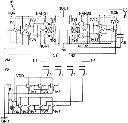
1. A charge pump circuit comprising:
a first capacitor including a first end to which a first voltage is supplied;
a second capacitor including a first end to which a first pulse signal is supplied, and a second end coupled to a first node;
a third capacitor including a first end to which the first pulse signal is supplied;
a first transistor including a first end coupled to a second end of the first capacitor, and a second end coupled to the first node;
a second transistor including a first end coupled to the first end of the first capacitor, and a second end coupled to the first node; and
a first circuit including a first input terminal coupled to the first node, a second input terminal coupled to a second end of the third capacitor, a first output terminal coupled to a gate of the first transistor, and a second output terminal coupled to a gate of the second transistor.
|