US 12,191,736 B2
Electronic device
Mikio Umehara, Yonago (JP); and Yutaka Kamogi, Yonago (JP)
Assigned to MINEBEA MITSUMI Inc., Nagano (JP)
Filed by Minebea Mitsumi Inc., Nagano (JP)
Filed on Oct. 18, 2023, as Appl. No. 18/489,238.
Application 17/237,782 is a division of application No. 16/906,260, filed on Jun. 19, 2020, granted, now 11,031,854, issued on Jun. 8, 2021.
Application 16/906,260 is a division of application No. 15/822,465, filed on Nov. 27, 2017, granted, now 10,727,726, issued on Jul. 28, 2020.
Application 18/489,238 is a continuation of application No. 18/057,428, filed on Nov. 21, 2022, granted, now 11,831,213.
Application 18/057,428 is a continuation of application No. 17/237,782, filed on Apr. 22, 2021, granted, now 11,539,278.
Claims priority of application No. 2016-230689 (JP), filed on Nov. 28, 2016.
Prior Publication US 2024/0072626 A1, Feb. 29, 2024
Int. Cl. H02K 33/02 (2006.01); G06F 3/01 (2006.01); H02K 5/22 (2006.01)
CPC H02K 33/02 (2013.01) [H02K 5/225 (2013.01); G06F 3/016 (2013.01)] 16 Claims
OG exemplary drawing
 
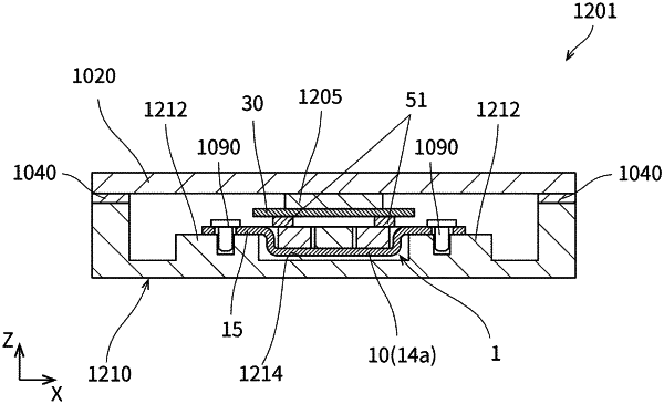
1. An electronic device, comprising:
a housing;
a touch panel attached to the housing;
a base attached to the housing;
a plate displaceable with respect to the base;
a plurality of elastic members supporting the plate with respect to the base; and
a coil inside the plurality of elastic members;
wherein
the touch panel, the base, the plate, and the elastic members are arranged inside the housing,
the coil is arranged in the plate side with respect to the base,
a magnetic gap is formed with the plate and the base, and
the plate connects with the touch panel in a winding axis direction of the coil.