| CPC H02H 3/08 (2013.01) [H02H 1/0007 (2013.01); H03K 5/24 (2013.01)] | 27 Claims |
|
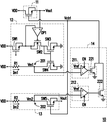
1. An overcurrent protection circuit, comprising:
a load switch, wherein two terminals thereof are respectively connected to a first voltage and a second voltage;
a first mirror circuit connected to the load switch;
a second mirror circuit connected to the load switch;
a control circuit connected to the load switch, the first mirror circuit, and the second mirror circuit,
wherein the first mirror circuit is configured to detect whether there is an overcurrent in a current flowing through the load switch in a state that a voltage difference between the two terminals of the load switch is within a first voltage region,
the first mirror circuit is configured to generate a first node voltage in the state that the voltage difference between the two terminals of the load switch is within the first voltage region,
the second mirror circuit is configured to detect whether there is the overcurrent in the current flowing through the load switch in a state that the voltage difference between the two terminals of the load switch is within a second voltage region,
the second mirror circuit is configured to generate a second node voltage in the state that the voltage difference between the two terminals of the load switch is within the second voltage region,
the control circuit is configured to cut off the load switch according to at least one of the first node voltage and the second node voltage to perform an overcurrent protection, and
the first voltage region covers a portion of a voltage range between a drive voltage and a reference ground voltage, the second voltage region covers an another portion of the voltage range between the drive voltage and the reference ground voltage, and the first voltage region and the second voltage region are at least partially overlapped,
wherein the first mirror circuit comprises:
a first current mirror circuit connected to the load switch, wherein the second mirror circuit comprises:
a second current mirror circuit connected to the load switch
wherein the first current mirror circuit is configured to generate a first mirror current according to the current flowing through the load switch,
wherein the second current mirror circuit is configured to generate a second mirror current according to the current flowing through the load switch.
|