| CPC H01P 3/12 (2013.01) [H01L 23/3107 (2013.01); H01L 25/18 (2013.01); H05K 1/181 (2013.01)] | 20 Claims |

|
1. A package, comprising:
a semiconductor die having a first surface and a second surface opposing the first surface, the semiconductor die including circuitry formed in the first surface;
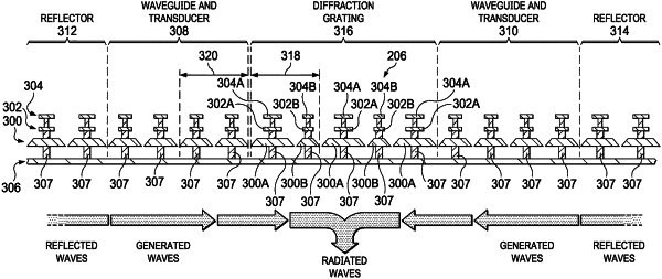
an acoustic waveguide in the semiconductor die, the acoustic waveguide including an array of capacitors, the array of capacitors including a transducer portion and a diffraction grating portion, the transducer portion configured to convert signals between electrical signals and acoustic waves, the diffraction grating portion configured to direct the acoustic waves toward and receive the acoustic waves from the second surface; and
a connector coupling the circuitry to the acoustic waveguide.
|