| CPC H01L 33/62 (2013.01) [H01L 23/49541 (2013.01); H01L 33/486 (2013.01); H01L 33/52 (2013.01); H01L 33/54 (2013.01); H01L 33/56 (2013.01); H01L 33/60 (2013.01); H01L 33/642 (2013.01); H01L 33/647 (2013.01); H01L 2224/48247 (2013.01); H01L 2224/48465 (2013.01)] | 9 Claims |
|
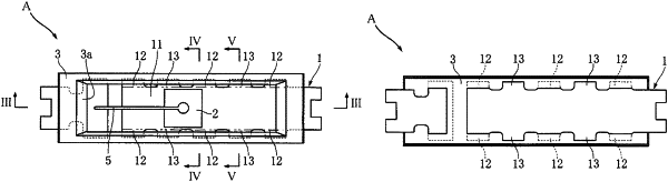
1. A semiconductor device comprising:
a first portion of a lead frame including a bonding portion;
a second portion of a lead frame spaced apart from the first portion of lead frame in a first direction perpendicular to a thickness direction of the bonding portion;
a semiconductor element mounted on a first surface of the bonding portion and electrically connected to the first portion of lead frame and the second portion of lead frame; and
a case covering a part of the first portion of lead frame and a part of the second portion of lead frame,
wherein the bonding portion includes a first exposed surface that is opposite from the first surface and exposed from the case,
the first portion of lead frame further includes a plurality of thin extensions and a plurality of thick extensions, each thin extension extending from the bonding portion in a second direction perpendicular to the thickness direction and the first direction, each thin extension being smaller in thickness than the bonding portion, and each thick extension extending from the bonding portion in the second direction,
the plurality of thick extensions are disposed next to the plurality of thin extensions and have a same thickness as the bonding portion, each thick extension including a second exposed surface that is exposed from the case,
the second exposed surface of each thick extension and the first exposed surface of the bonding portion are contained in a same flat plane, and
the positions of the plurality of thick extensions are at different locations in the first direction from the positions of the plurality of thin extensions.
|