| CPC H01L 33/502 (2013.01) [H01L 27/156 (2013.01); H01L 33/52 (2013.01)] | 14 Claims |

|
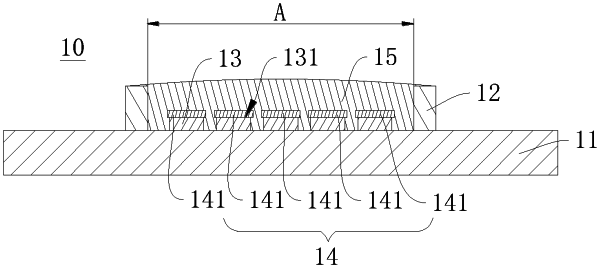
1. A chip-on-board (COB) type photoelectric device, comprising:
a metallic substrate, comprising: a photoelectric element fixing area;
a dam, disposed on the metallic substrate and surrounding the photoelectric element fixing area;
a plurality of first photoelectric elements, disposed on the metallic substrate and in the photoelectric element fixing area;
a KSF phosphor based layer, disposed on the plurality of first photoelectric elements and being not in contact with the metallic substrate, wherein the KSF phosphor based layer comprises a KSF phosphor; and
an isolation layer, disposed in the dam and covering the KSF phosphor based layer; wherein the isolation layer comprises:
a first isolation layer, disposed on the metallic substrate, and a height of the first isolation layer in a direction perpendicular to the metallic substrate is not higher than a height of each of the plurality of first photoelectric elements in the direction perpendicular to the metallic substrate; and
a second isolation layer, disposed over the KSF phosphor based layer.
|