| CPC H01L 33/387 (2013.01) [H01L 25/0753 (2013.01); H01L 27/156 (2013.01); H01L 33/005 (2013.01); H01L 33/505 (2013.01); H01L 33/62 (2013.01); H01L 2933/0016 (2013.01); H01L 2933/0066 (2013.01)] | 20 Claims |

|
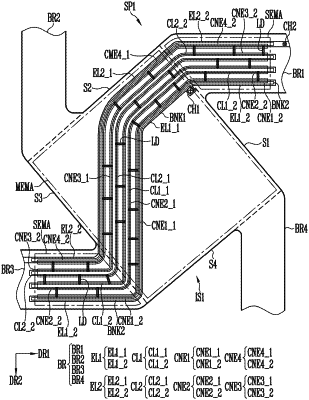
1. A display device comprising:
a base layer comprising a plurality of islands, at least one first bridge configured to connect the islands in a first direction, and at least one second bridge configured to connect the islands in a second direction; and
at least one pixel comprising a plurality of sub-pixels in the base layer,
wherein each of the sub-pixels comprises:
a first electrode and a second electrode in one island of the islands and spaced from each other;
a third electrode and a fourth electrode in one bridge of the at least one first bridge and the at least one second bridge and spaced from each other;
at least one first light emitting element between the first electrode and the second electrode; and
at least one second light emitting element between the third electrode and the fourth electrode.
|