| CPC H01L 33/382 (2013.01) [H01L 33/0095 (2013.01); H01L 33/54 (2013.01); H01L 2933/0016 (2013.01); H01L 2933/005 (2013.01)] | 9 Claims |

|
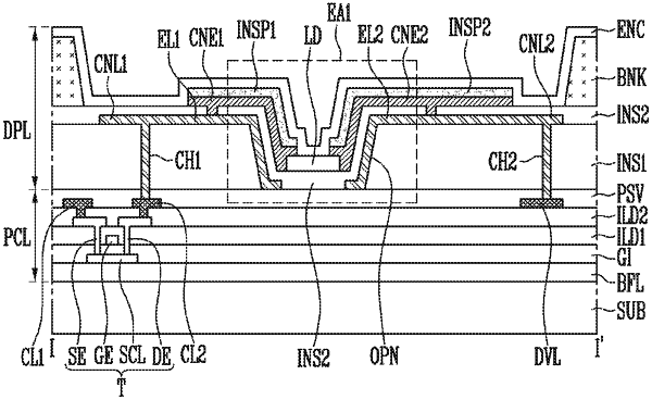
1. A display device comprising:
a substrate having a display area and a non-display area extending around a side of the display area, the display area comprising a plurality of pixel areas; and
a pixel in each of the pixel areas, the pixel comprising:
an insulating layer on a surface of the substrate and having an opening;
first and second electrodes on the insulating layer and spaced apart from each other;
a plurality of light emitting elements in the opening;
a first contact electrode electrically connecting one end of the light emitting elements and the first electrode to each other;
a second contact electrode electrically connecting another end of the light emitting elements and the second electrode to each other;
a first insulating pattern on the first contact electrode; and
a second insulating pattern on the second contact electrode, the first insulating pattern and the second insulating pattern being on the same layer and spaced apart from each other in a direction parallel to the surface of the substrate such that the first insulating pattern and the second insulating pattern do not overlap each other when viewed on a plane.
|