| CPC H01L 33/382 (2013.01) [H01L 33/0075 (2013.01); H01L 33/08 (2013.01)] | 18 Claims |
|
1. An optoelectronic semiconductor device, comprising:
a first semiconductor layer stack comprising a first semiconductor layer of a first conductivity type, wherein a layer which is directly adjacent to a first main surface of the first semiconductor stack is epitaxial,
the optoelectronic semiconductor device further comprising a second semiconductor layer of a second conductivity type,
a first contact element and a second contact element,
wherein the first semiconductor layer stack and the second semiconductor layer are arranged one above the other,
the second semiconductor layer is electrically connected to the second contact element, and
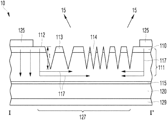
wherein part of the first main surface of the first semiconductor layer stack is directly adjacent to the first contact element and part of the first main surface of the first semiconductor layer stack is patterned so that a plurality of protruding regions and a plurality of connecting regions are formed, the connecting regions being directly adjacent to regions in which part of the first main surface of the first semiconductor layer stack is directly adjacent to the first contact element, and the connecting regions having a lateral extension which is greater than 5 times the mean lateral extension of the protruding regions,
wherein at least one of the connecting regions is a light emitting region that is not covered with a conductive material.
|