| CPC H01L 33/20 (2013.01) [H01L 27/156 (2013.01); H01L 33/005 (2013.01); H01L 33/382 (2013.01)] | 16 Claims |

|
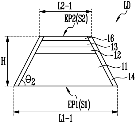
1. A light emitting element comprising:
a first surface corresponding to an end of the light emitting element;
a second surface corresponding to another end of the light emitting element;
a first semiconductor layer adjacent to the first surface, the first semiconductor layer including a first type of semiconductor;
a second semiconductor layer adjacent to the second surface, the second semiconductor layer including a second type of semiconductor different from the first type of semiconductor;
a transparent electrode between the second semiconductor layer and the second surface;
an active layer disposed between the first semiconductor layer and the second semiconductor layer; and
an insulating film that overlaps the first semiconductor layer, the active layer, the second semiconductor layer, and the transparent electrode so that sides of the first semiconductor layer, the active layer, and the second semiconductor layer, and the transparent electrode are prevented from being exposed to the outside, wherein
a thickness of the insulating film is from about 10 nm to about 200 nm,
an area of the first surface is larger than an area of the second surface,
a distance between the first surface and the second surface is shorter than a length defined by the first surface,
the first surface and the second surface each have an n-polygonal shape (n is an integer of 3 or more), and
the length defined by the first surface is defined by the following equation;
L=√x×y, where L is the length defined by the first surface, x is a diameter of an inscribed circle with respect to the first surface, and y is a diameter of a circumscribed circle with respect to the first surface.
|