| CPC H01L 31/0321 (2013.01) [H01L 31/18 (2013.01); H01L 31/1884 (2013.01)] | 17 Claims |

|
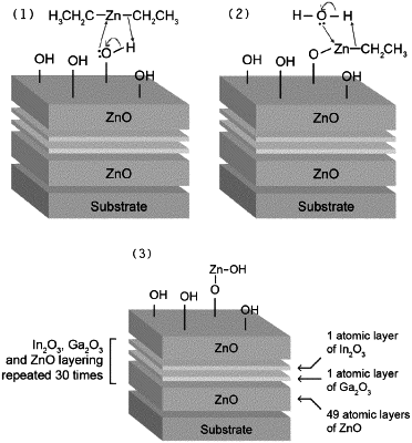
1. A method for doping an oxide semiconductor material, wherein the method comprises:
(i) depositing a first single atomic layer of a first oxide semiconductor on a substrate;
(ii) depositing at least a second single atomic layer of the first oxide semiconductor directly on the first single atomic layer to form a plurality of atomic layers of the first oxide semiconductor on the substrate; and
(iii) depositing one atomic layer of a first dopant material on the plurality of atomic layers of the first oxide semiconductor using H2O as an oxidant to obtain a doped oxide semiconductor material, wherein the first dopant material comprises gallium or indium;
(iv) depositing one atomic layer of a second dopant material directly on the one atomic layer of the first dopant material; and
(v) repeating steps (i)-(iv) so as to obtain a doped oxide semiconductor material, wherein the doped oxide semiconductor material is a film having the first dopant material present in an amount of about 1 at % and the second dopant material present in an amount of about 1 at %.
|