| CPC H01L 31/02167 (2013.01) [H01L 31/022425 (2013.01); H01L 31/068 (2013.01); H01L 31/1868 (2013.01); Y02E 10/547 (2013.01); Y02P 70/50 (2015.11)] | 7 Claims |

|
1. A solar cell comprising:
a semiconductor substrate of a p-type which has a pn junction and has an n-type layer on a light receiving surface of the semiconductor substrate on one side thereof and a non-light receiving surface on another side thereof;
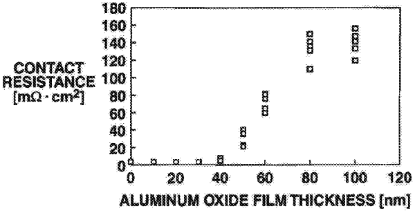
a passivation layer consisting essentially of an amorphous aluminum oxide and having a thickness of 1 to 20 nm in contact with the p-type substrate in the non-light receiving surface of the semiconductor substrate;
a first dielectric film of a material selected from the group consisting of silicon nitride, silicon oxide, silicon carbide and titanium oxide on the passivation layer;
a second dielectric film of a material selected from the group consisting of silicon nitride, silicon oxide, silicon carbide and titanium oxide on the light receiving surface of the semiconductor substrate;
a first power extraction electrode on said non-light receiving surface which is a sintered product of a first conductive metal paste containing silver powder, glass frit and organic binder wherein the first power extraction electrode is in electrical contact with the p-type surface of the semiconductor substrate by firing-through the first dielectric film and the passivation layer; and
a second power extraction electrode on said light receiving surface which is a sintered product of a second conductive metal paste containing silver powder, glass frit and organic binder wherein the second power extraction electrode is in electrical contact with the n-type layer of the semiconductor substrate by firing-through the second dielectric film,
wherein the first and second electrodes contain at least one element selected from the group consisting of B, Na, K, Ca, Si, V, Zn, Zr, Cd, Sn, Ba, Ta, Tl, Pb and Bi.
|