| CPC H01L 29/84 (2013.01) [H01L 21/30625 (2013.01); H01L 21/76843 (2013.01)] | 10 Claims |

|
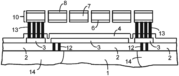
1. A method for producing a semiconductor transducer device, the method comprising:
providing a semiconductor body;
forming a sacrificial layer above a surface of the semiconductor body;
applying a diaphragm on the sacrificial layer; and
removing the sacrificial layer by introducing an etchant into openings of the diaphragm,
wherein applying the diaphragm comprises:
applying a first layer comprising tungsten, wherein the first layer is a layer of a finished diaphragm with a largest thickness,
reducing a roughness of a surface of the first layer facing away from the semiconductor body thereby providing a processed surface, and
patterning and structuring the first layer to form the openings,
wherein applying the diaphragm comprises applying a third layer comprising at least one of titanium or titanium nitride,
wherein the first layer is applied on a surface of the third layer facing away from the semiconductor body, and
wherein the processed surface has a roughness profile with an arithmetic average between 2 nm and 10 nm inclusive.
|