| CPC H01L 29/7869 (2013.01) [H01L 29/78618 (2013.01); H01L 29/78645 (2013.01); H01L 29/78696 (2013.01)] | 15 Claims |
|
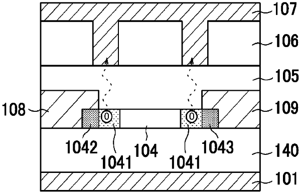
1. A semiconductor device having TFT using an oxide semiconductor comprising:
the oxide semiconductor including a channel region, a source region, a drain region, and a transition region between the channel region and the source region and between the channel region and the drain region, wherein
a resistivity of the transition region is smaller than that of the channel region, and larger than that of the source region or the drain region,
a source electrode is formed overlapping the source region, and a drain electrode is formed overlapping the drain region,
a thickness of the transition region of the oxide semiconductor is larger than a thickness of the channel region of the oxide semiconductor,
a first gate insulating film covers the oxide semiconductor,
a second gate insulating film covers the first gate insulating film,
a through hole is formed in the second gate insulating film at a place corresponding to the transition region of the oxide semiconductor, and
a gate electrode is formed covering the second gate insulating film and the through hole.
|