| CPC H01L 29/7869 (2013.01) [H01L 29/78618 (2013.01)] | 12 Claims |
|
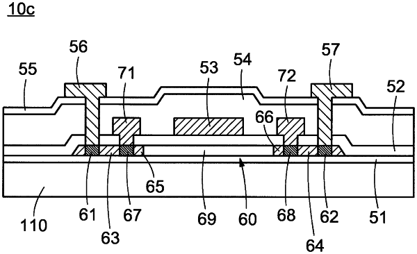
1. A semiconductor device including a thin-film transistor, the thin-film transistor comprising:
an oxide semiconductor layer;
a gate insulating layer;
a gate electrode overlapped on the oxide semiconductor layer through the gate insulating layer;
a source electrode in contact with the oxide semiconductor layer;
a drain electrode in contact with the oxide semiconductor layer; and
a first metal layer in contact with the oxide semiconductor layer and disposed between the source electrode and the drain electrode at a distance from the source electrode and the drain electrode, wherein
the oxide semiconductor layer includes a channel region and a low resistance region, the low resistance region overlaps the first metal layer, and
an oxygen concentration of the low resistance region is lower than the oxygen concentration of the channel region.
|