| CPC H01L 29/78618 (2013.01) [H01L 21/02532 (2013.01); H01L 21/0259 (2013.01); H01L 21/823807 (2013.01); H01L 21/823814 (2013.01); H01L 21/823864 (2013.01); H01L 27/092 (2013.01); H01L 29/0665 (2013.01); H01L 29/42392 (2013.01); H01L 29/66553 (2013.01); H01L 29/66636 (2013.01); H01L 29/66742 (2013.01); H01L 29/7848 (2013.01); H01L 29/78696 (2013.01)] | 20 Claims |

|
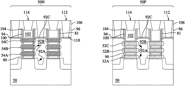
1. A nano-FET comprising:
a substrate, the substrate comprising a fin;
isolation regions over the substrate and along opposing sides of the fin;
a plurality of first nanostructures over the fin;
an epitaxial source/drain region adjacent the plurality of first nanostructures, the epitaxial source/drain region comprises:
a first semiconductor material layer comprising first semiconductor material segments and a second semiconductor material segment, each of the first semiconductor material segments contacting an end of at least one of the plurality of first nanostructures, each of the first semiconductor material segments being separated from others of the first semiconductor material segments, the first semiconductor material segments having a first dopant concentration of dopants of a first conductivity type; and
a second semiconductor material layer having a second dopant concentration of dopants of the first conductivity type, the second dopant concentration being greater than the first dopant concentration, the second semiconductor material layer comprising a single layer covering each of the first semiconductor material segments; and
a gate electrode over the plurality of first nanostructures;
wherein each of the first semiconductor material segments have a first thickness, each of the plurality of first nanostructures have a second thickness, the first thickness is greater than the second thickness for each first semiconductor material segment in contact with the end of the at least one of the plurality of first nanostructures, each nanostructure of the plurality of first nanostructures being separated by the gate electrode, a spacer is disposed between the gate electrode and the epitaxial source/drain region, the spacer being further disposed between adjacent nanostructures of the plurality of first nanostructures, and an interface between each nanostructure of the plurality of first nanostructures and each of the first semiconductor material segments having a shape curving outwards towards the epitaxial source drain region at the center; and
wherein the second semiconductor material segment is on a recessed portion of the substrate adjacent to the fin, the second semiconductor material segment is discontinuous from the first semiconductor material segments, the second semiconductor material segment has the first dopant concentration of the first conductivity type.
|