US 12,191,386 B2
Power semiconductor device and method of fabricating the same
Jeong Mok Ha, Yongin-si (KR); Hyuk Woo, Yongin-si (KR); Sin A Kim, Yongin-si (KR); Tae Youp Kim, Yongin-si (KR); Ju Hwan Lee, Yongin-si (KR); Min Gi Kang, Yongin-si (KR); and Tae Yang Kim, Yongin-si (KR)
Assigned to HYUNDAI MOBIS CO., LTD., Seoul (KR)
Filed by HYUNDAI MOBIS CO., LTD., Seoul (KR)
Filed on Mar. 13, 2024, as Appl. No. 18/603,723.
Application 18/603,723 is a continuation of application No. 17/330,039, filed on May 25, 2021, granted, now 11,961,903.
Claims priority of application No. 10-2020-0063131 (KR), filed on May 26, 2020; application No. 10-2020-0064148 (KR), filed on May 28, 2020; application No. 10-2020-0066309 (KR), filed on Jun. 2, 2020; application No. 10-2020-0068205 (KR), filed on Jun. 5, 2020; application No. 10-2020-0069417 (KR), filed on Jun. 9, 2020; application No. 10-2020-0070701 (KR), filed on Jun. 11, 2020; application No. 10-2020-0071310 (KR), filed on Jun. 12, 2020; and application No. 10-2020-0144559 (KR), filed on Nov. 2, 2020.
Prior Publication US 2024/0222497 A1, Jul. 4, 2024
Int. Cl. H01L 29/78 (2006.01); H01L 29/16 (2006.01); H01L 29/66 (2006.01)
CPC H01L 29/7813 (2013.01) [H01L 29/1608 (2013.01); H01L 29/66734 (2013.01)] 15 Claims
OG exemplary drawing
 
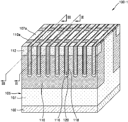
1. A power semiconductor device comprising:
a first trench recessed into a semiconductor layer in a first direction from a surface of the semiconductor layer and extending in a second direction which is different from the first direction;
a source contact region spaced apart from the first trench in the second direction;
a well region including a first well region which is in contact with the first trench and a second well region which is in contact with the first trench and is spaced apart from the first well region; and
a drift region including a vertical portion of the drift region which is in contact with the first trench and is disposed between the first well region and the second well region;
wherein the vertical portion of the drift region is in contact with the surface of the semiconductor layer.