| CPC H01L 29/66818 (2013.01) [H01L 21/02532 (2013.01); H01L 21/02603 (2013.01); H01L 21/823807 (2013.01); H01L 21/823814 (2013.01); H01L 21/823821 (2013.01); H01L 21/823828 (2013.01); H01L 21/823871 (2013.01); H01L 27/092 (2013.01); H01L 27/0924 (2013.01); H01L 29/0673 (2013.01); H01L 29/0847 (2013.01); H01L 29/1037 (2013.01); H01L 29/161 (2013.01); H01L 29/42392 (2013.01); H01L 29/66545 (2013.01); H01L 29/66742 (2013.01); H01L 29/7848 (2013.01); H01L 29/78618 (2013.01); H01L 29/78684 (2013.01); H01L 29/78696 (2013.01)] | 20 Claims |

|
1. A method comprising:
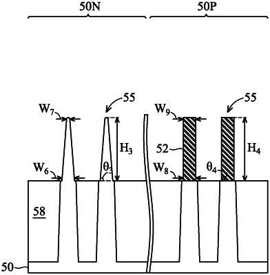
forming a semiconductor fin over a semiconductor substrate, the semiconductor fin comprising a silicon germanium portion and a silicon portion, wherein a germanium concentration of a lower portion of the silicon germanium portion of the semiconductor fin is greater than a germanium concentration of an upper portion of the silicon germanium portion of the semiconductor fin; and
trimming the semiconductor fin, wherein the lower portion of the silicon germanium portion of the semiconductor fin is trimmed at a greater rate than the upper portion of the silicon germanium portion of the semiconductor fin, wherein trimming the semiconductor fin exposes a first horizontal surface of the silicon portion of the semiconductor fin.
|