| CPC H01L 29/4991 (2013.01) [H01L 21/764 (2013.01); H01L 27/0886 (2013.01); H01L 29/0673 (2013.01); H01L 29/41733 (2013.01); H01L 29/41791 (2013.01); H01L 29/42392 (2013.01); H01L 29/4908 (2013.01); H01L 29/66545 (2013.01); H01L 29/6656 (2013.01); H01L 29/66795 (2013.01); H01L 29/7851 (2013.01); H01L 29/78696 (2013.01)] | 20 Claims |

|
1. A method of manufacturing a semiconductor device, the method comprising:
forming an active region protruding from a substrate and extending in a first direction;
forming a sacrificial gate structure on the active region and extending a second direction perpendicular to the first direction;
forming a first spacer, a second spacer, and a sacrificial spacer between the first spacer and the second spacer on at least one side of the sacrificial gate structure;
forming a recess region by removing a portion of the active region on the at least one side of the sacrificial gate structure;
forming a source/drain region on the recess region;
forming a first insulating layer on the source/drain region;
forming an air-gap spacer by removing the sacrificial spacer with respect to the first spacer and the second spacer;
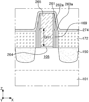
forming a liner layer on the first insulating layer and the second spacer so that an upper portion of the second spacer is bent towards an upper portion of the first spacer to cap the air-gap spacer;
removing the liner layer;
forming a second insulating layer on the first insulating layer and the second spacer;
forming a gap region by removing the sacrificial gate structure; and
forming a gate structure by depositing a gate dielectric layer, a gate electrode, and a gate capping layer in the gap region.
|
|
12. A method of manufacturing a semiconductor device, the method comprising:
forming a sacrificial gate structure on a substrate;
forming a spacer structure on sides of the sacrificial gate structure; and
forming an insulating structure on sides of the spacer structure,
wherein forming the spacer structure comprises:
forming first spacers on the sides of the sacrificial gate structure;
forming sacrificial spacers on external sides of the first spacers;
forming second spacers on external sides of the sacrificial spacers; and
forming air-gap spacers by removing the sacrificial spacers with respect to the first spacers and the second spacers,
wherein forming the insulating structure comprises:
forming a first insulating layer on the sides of the spacer structure after forming the second spacers;
forming a liner layer on the first insulating layer after forming the air-gap spacers so that an upper portion of each of the second spacers is bent towards an upper portion of each of the first spacers;
removing the liner layer; and
forming a second insulating layer on the first insulating layer.
|
|
19. A method of manufacturing a semiconductor device, the method comprising:
forming an active region on a substrate;
forming a sacrificial gate structure on the active region;
forming a spacer structure including a first spacer, a second spacer, and an air-gap spacer between the first spacer and the second spacer;
forming source/drain regions on the active region and on both sides of the sacrificial gate structure;
forming an insulating structure on the sides of the spacer structure and the source/drain regions;
forming a liner layer on the insulating structure and the second spacer so that the upper portion of the second spacer is bent toward the upper portion of the first spacer to cap the air gap spacer;
removing the liner layer;
forming a gap region by removing the sacrificial gate structure; and
forming a gate structure by depositing a gate dielectric layer, a gate electrode, and a gate capping layer in the gap region,
wherein the upper portion of the second spacer is in physical contact with the upper portion of the first spacer on a contact surface,
wherein a lowermost end of the contact surface is on a level higher than an upper surface of the gate electrode with the substrate being a reference base level, and
wherein an uppermost end of the air-gap spacer is on a level higher than the upper surface of the gate electrode with the substrate being a reference base level.
|