| CPC H01L 29/42392 (2013.01) [H01L 29/0665 (2013.01); H01L 29/41775 (2013.01); H01L 29/66553 (2013.01); H01L 29/78696 (2013.01)] | 20 Claims |

|
1. A method, comprising:
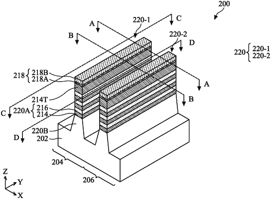
forming a stack of channel layers and sacrificial layers on a substrate, the channel layers and the sacrificial layers having different material compositions and being alternatingly disposed in a vertical direction;
patterning the stack to form a semiconductor fin;
forming an isolation feature on sidewalls of the semiconductor fin;
recessing the semiconductor fin, thereby forming a source/drain recess, such that a recessed top surface of the semiconductor fin is below a top surface of the isolation feature;
growing a base epitaxial layer from the recessed top surface of the semiconductor fin;
depositing an insulation layer in the source/drain recess, wherein the insulation layer is above the base epitaxial layer and above a bottommost channel layer; and
forming an epitaxial feature in the source/drain recess, wherein the epitaxial feature is above the insulation layer.
|