| CPC H01L 29/42392 (2013.01) [H01L 27/088 (2013.01); H01L 29/41733 (2013.01); H01L 29/78696 (2013.01)] | 20 Claims |

|
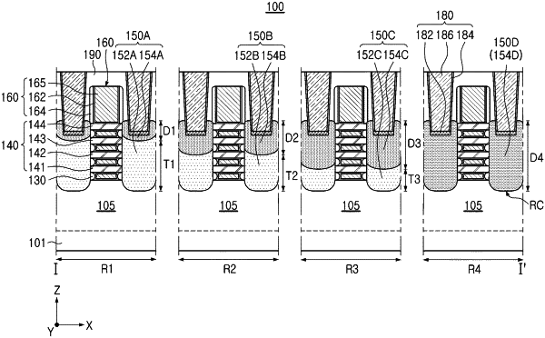
1. A semiconductor device comprising:
active regions extending on a substrate in a first direction;
first and second gate structures intersecting the active regions and extending on the substrate in a second direction;
a plurality of channel layers spaced apart from each other in a third direction, perpendicular to an upper surface of the substrate, on the active regions and surrounded in the second and third directions by the first and second gate structures;
first and second source/drain regions in recess regions in which the active regions are recessed on at least one side of each of the first and second gate structures, and physically contacting the plurality of channel layers; and
contact plugs connected to the first and second source/drain regions,
wherein each of the first and second source/drain regions includes:
a first epitaxial layer on each of the active regions in each of the recess regions; and
a second epitaxial layer on the first epitaxial layer and including first conductivity-type impurities,
the first epitaxial layer has a maximum first thickness in the third direction in the first source/drain region, and
the first epitaxial layer has a maximum second thickness less than the maximum first thickness in the third direction in the second source/drain region.
|