| CPC H01L 29/42368 (2013.01) [H01L 21/76224 (2013.01); H01L 21/823462 (2013.01); H01L 29/401 (2013.01); H01L 29/4236 (2013.01); H01L 29/7813 (2013.01); H01L 29/7825 (2013.01); H01L 29/7834 (2013.01)] | 20 Claims |
|
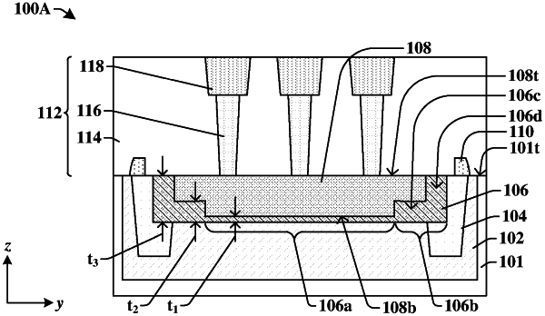
1. A semiconductor device comprising:
a first doped region arranged within a semiconductor substrate, the first doped region having a first doping conductivity;
a second doped region and a third doped region arranged within the semiconductor substrate on opposite sides of the first doped region, the second doped region and third doped region spaced apart from one another in a first direction and having a second doping conductivity opposite the first doping conductivity;
a gate electrode arranged over the first doped region, the gate electrode comprising a bottom surface arranged below a topmost surface of the semiconductor substrate;
a trench isolation structure surrounding the second doped region, the third doped region, and the gate electrode; and
a gate dielectric structure separating the gate electrode from the first doped region, wherein when viewed in cross-section along a second direction perpendicular to the first direction the gate dielectric structure comprises a central portion having a first thickness and a corner portion having a second thickness greater than the first thickness;
wherein the gate dielectric structure has a third thickness from an outer sidewall of the corner portion to an outer sidewall of the gate electrode, the third thickness being measured in the second direction;
wherein the third thickness is in a range between twenty percent and one percent of a distance between outermost sidewalls of the gate dielectric structure.
|