| CPC H01L 29/4236 (2013.01) [H10B 12/0335 (2023.02); H10B 12/053 (2023.02); H10B 12/34 (2023.02)] | 22 Claims |

|
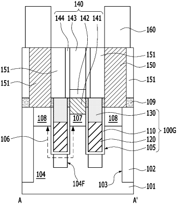
1. A semiconductor device, comprising:
a substrate;
a first fluorine-containing layer over the substrate;
a trench formed in the first fluorine-containing layer and extended into the substrate;
a gate dielectric layer formed over the trench;
a gate electrode formed over the gate dielectric layer and filling a portion of the trench;
a second fluorine-containing layer formed over to directly contact the gate electrode; and
a fluorine-containing passivation layer between the gate dielectric layer and the gate electrode,
wherein a bottom surface of the first fluorine-containing layer covers a top surface of the gate dielectric layer and a top surface of the fluorine-containing passivation layer.
|