| CPC H01L 29/401 (2013.01) [H01L 21/049 (2013.01); H01L 29/1608 (2013.01); H01L 29/4236 (2013.01)] | 20 Claims |
|
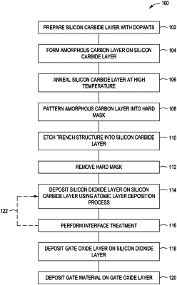
1. A method of forming a gate structure on a substrate, comprising:
depositing an amorphous carbon layer on a silicon carbide layer of the gate structure on the substrate to form a capping layer on the silicon carbide layer;
annealing the silicon carbide layer at a temperature of greater than approximately 1800 degrees Celsius;
forming a hard mask on the silicon carbide layer by patterning the amorphous carbon layer;
etching a trench structure of the gate structure into the silicon carbide layer using the hard mask;
removing the hard mask to expose the silicon carbide layer;
depositing a silicon dioxide layer of the gate structure on the silicon carbide layer using an atomic layer deposition process;
performing at least one interface treatment on the silicon dioxide layer;
depositing a gate oxide layer of the gate structure on the silicon dioxide layer; and
depositing a gate material of the gate structure on the gate oxide layer.
|