| CPC H01L 29/0847 (2013.01) [H01L 21/02595 (2013.01); H01L 21/02686 (2013.01); H01L 29/04 (2013.01); H01L 29/0684 (2013.01); H01L 29/66666 (2013.01); H01L 29/7827 (2013.01)] | 7 Claims |
|
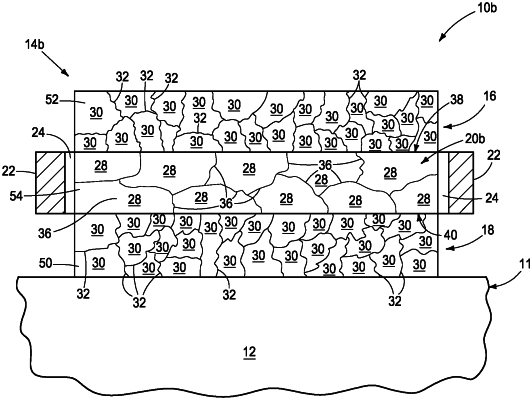
1. A vertical transistor comprising:
a top source/drain region, a bottom source/drain region, a channel region vertically between the top and bottom source/drain regions, and a gate operatively laterally-adjacent the channel region;
the top and bottom source/drain regions having polycrystalline crystal grains and grain boundaries between immediately-adjacent of the polycrystalline crystal grains; the channel region having channel crystal grains having a first average crystal grain size and comprising grain boundaries between immediately-adjacent of the channel crystal grains, the top source/drain region having a second average crystal grain size, and the bottom source/drain region having a third average crystal grain size that differs from the second average crystal grain size;
the top source/drain region and the channel region having a top interface and the bottom source/drain region and the channel region having a bottom interface;
at least 50% of the grain boundaries in the top source/drain region at the top interface being laterally offset from the grain boundaries of the channel crystal grains in the channel region at the top interface; and
at least 50% of the grain boundaries in the bottom source/drain region at the bottom interface being laterally offset from the grain boundaries of the channel crystal grains in the channel region at the bottom interface.
|