| CPC H01L 29/0607 (2013.01) [H01L 27/0886 (2013.01); H01L 29/0653 (2013.01); H01L 29/0673 (2013.01); H01L 29/0847 (2013.01); H01L 29/161 (2013.01); H01L 29/201 (2013.01); H01L 29/205 (2013.01); H01L 29/42392 (2013.01); H01L 29/775 (2013.01); H01L 29/785 (2013.01); H01L 29/78618 (2013.01); H01L 29/78696 (2013.01); H01L 21/823814 (2013.01); H01L 27/0924 (2013.01); H01L 29/66545 (2013.01)] | 25 Claims |

|
1. An integrated circuit device comprising:
a body above a substrate, the body having a top surface and a bottom surface opposite the top surface, the body comprising a first semiconductor material having a first band gap between a conduction band and a valence band of the first semiconductor material;
an insulation structure between the substrate and the bottom surface of the body;
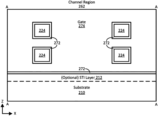
a gate structure including a gate dielectric structure having a portion on the body and a portion on the insulation structure, wherein the portion of the gate dielectric structure on the insulation structure is continuous along the insulation structure beneath the bottom surface of the body, the gate structure further including a gate electrode structure on the gate dielectric structure, wherein the gate structure is completely wrapped around a channel region of the body; and
a source region and a drain region, the body between the source region and the drain region, wherein at least one of the source region and the drain region comprises a second semiconductor material having a second band gap between a conduction band and a valence band of the second semiconductor material, the second band gap less than the first band gap of the body, and wherein the insulation structure extends vertically beneath the source region and the drain region.
|