| CPC H01L 28/55 (2013.01) [H01L 23/5223 (2013.01); H01L 28/40 (2013.01); H01L 28/60 (2013.01); H01L 28/86 (2013.01); H01L 28/90 (2013.01); H01L 28/91 (2013.01); H01L 28/92 (2013.01)] | 20 Claims |

|
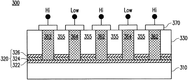
1. A semiconductor device, comprising:
an insulation layer; and
a dielectric layer comprising:
a first electrode with sidewalls and a bottom surface in contact with the insulation layer,
a second electrode with sidewalls and a bottom surface in contact with the insulation layer, and
an insulator formed between the first electrode and the second electrode, wherein the insulator is coupled to a sidewall of the first electrode and coupled to a sidewall of the second electrode, wherein:
the first electrode is electrically connected to a first voltage,
the second electrode is electrically connected to a second voltage different from the first voltage, and wherein:
the bottom surface of the first electrode has a first shape;
the bottom surface of the second electrode has a second shape; and
the first shape and the second shape have same dimensions and a same area,
the first electrodes are electrically connected to a first voltage via the at least one metal layer;
the second electrodes are electrically connected to a second voltage via the at least one metal layer; and
the first voltage is higher than the second voltage.
|