| CPC H01L 28/20 (2013.01) [H01L 27/0629 (2013.01); H01L 23/5286 (2013.01); H01L 27/092 (2013.01); H01L 27/0924 (2013.01)] | 14 Claims |

|
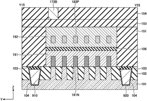
1. A semiconductor device comprising:
a substrate;
a first semiconductor region formed over the substrate;
a second semiconductor region formed over the substrate, and electrically connected to the first semiconductor region;
a third semiconductor region formed over the substrate, and positioned between the first semiconductor region and the second semiconductor region;
a fourth semiconductor region formed over the first semiconductor region;
a fifth semiconductor region formed over the second semiconductor region, and electrically connected to the fourth semiconductor region;
a sixth semiconductor region formed over the third semiconductor region, and positioned between the fourth semiconductor region and the fifth semiconductor region; and
wires formed between the first semiconductor region and the second semiconductor region, and between the fourth semiconductor region and the fifth semiconductor region, to cover the third semiconductor region and the sixth semiconductor region, the wires including conductors, wherein
a part of the wires is located between the substrate and the third semiconductor region.
|