| CPC H01L 27/156 (2013.01) [H01L 33/005 (2013.01); H01L 33/50 (2013.01); H01L 33/58 (2013.01); H01L 33/60 (2013.01); H01L 33/62 (2013.01); H01L 2933/0041 (2013.01); H01L 2933/0058 (2013.01); H01L 2933/0066 (2013.01)] | 27 Claims |

|
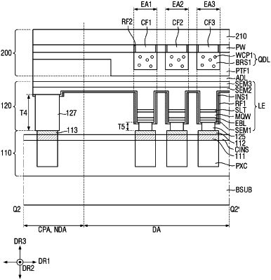
1. A display device comprising:
a plurality of light emitting elements on a first substrate;
a second substrate facing the first substrate;
a partition wall on one surface of the second substrate facing the first substrate, and including a plurality of openings;
a plurality of color filters in the plurality of openings;
wavelength conversion layers on the plurality of color filters, respectively, and configured to convert wavelengths of light emitted from the plurality of light emitting elements; and
an adhesive layer overlapping with the plurality of light emitting elements in a thickness direction, and located between the wavelength conversion layers and the light emitting elements in the thickness direction to adhere the first substrate and the second substrate to each other,
wherein the partition wall comprises a silicon single crystal.
|